PRODUCT

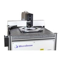
MicroSense

MicroSense DNA

MicroSense Wafer Geometry Measurement

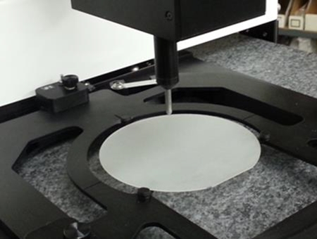
MicroSense capacitance sensor based metrology systems perform full wafer mapping, generating high resolution geometry data for each wafer.
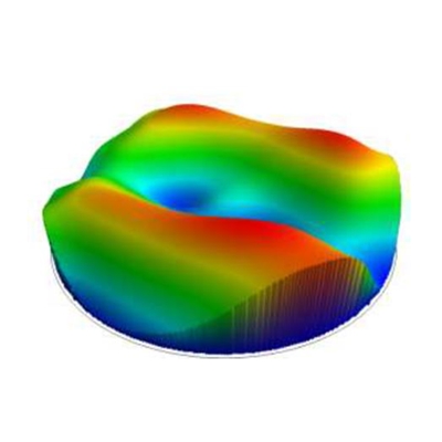
Wafer metrics include thickness, flatness, bow and warp.
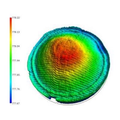
Thickness, Flatness
Bow, Warp
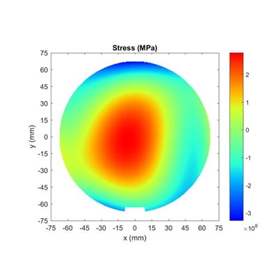
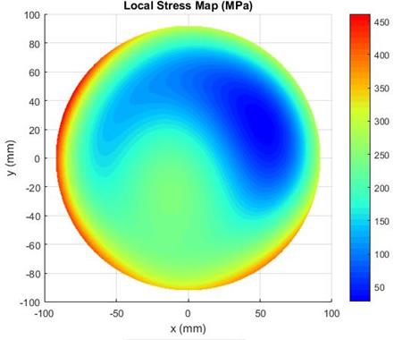
Thin Film Stress

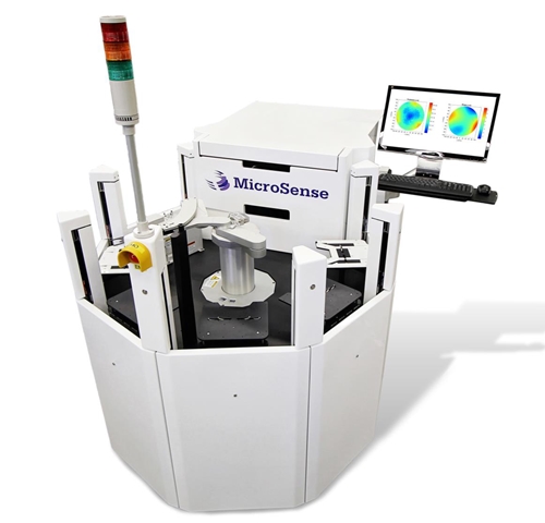
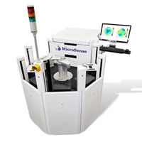
New UltraMap C200L 200mm Bare Silicon Wafer Geometry System

UMA-C200L
Measurement Technology Capacitance
(industry baseline, same as ADE)
Measurements: Thickness, Flatness, SFQR (site flatness), Bow, Warp, Resistivity, P N Type
Applications: HVM Final Inspection of Bare and Epitaxial 200mm Silicon Wafers
Correlates to existing ADE results (QC Record) with Better than ADE Capability
> 1.25x throughput in smaller footprint
Higher resolution and greater repeatability
Much improved reliability and reduced downtime

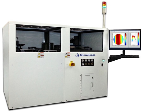
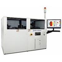
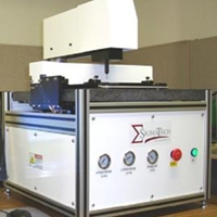
200mm Wafer Thin Film Stress Metrology System

UMA-C200-STR
Measurement Technology Capacitance
Measurements: Wafer Thickness and Shape, for Thin Film Stress Analysis
Applications: In process thin film stress monitoring of silicon, SiC and sapphire devicewafers.
Supports data handling for multiple deposition steps.
Correlates to existing Flexus results (QC Record) with Better than Flexus Capability
True full wafer 2D stress mapping
>120,000 measured data points per wafer
High throughput production tool

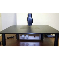
200mm Backgrind Device Wafer Thickness Metrology System

UMA-200-BP
Measurement Technology Backpressure
Measurements: Thickness and Flatness
Applications: Thickness and flatness monitoring of thinned backgrind wafers wafer only, wafer on carrier, wafer on tape
Material agnostic system silicon, SiC, sapphire, compound materials GaAs, InP
Measures ‹100 µm thick wafers

UltraMap 200mm Wafer Geometry Product Line

Application Thickness, Flatness, Shape Stress Backgrind Thickness
UMA-C200L
(200mm bare silicon wafers)
UMA-C200-STR
(150/200mm silicon full wafer stress)
UMA-200-BP
(150/200mm thinned back grind wafers, material independent)
Market Bare Wafer Manufacturing Device Manufacturing - Front End Device Manufacturing - Back End
Application Semi-auto benchtop Manual benchtop
UMS-C200B
(100/150/200mm silicon, SiC, sapphire)
UMS-200-BPBT
(100/150/200mm thinned back grind wafers, material independent)
UMM-BP1V-X30
(Up to 300mm, thinned back grind wafer)
Market Development & Low Volume Thinned wafer on film, Saw frame